This is a cautionary tale that will hopefully help someone else not fry their Submodule (I know, I know, I should have paid closer attention and also have done a few more tests before placing the SM onto my PCB.
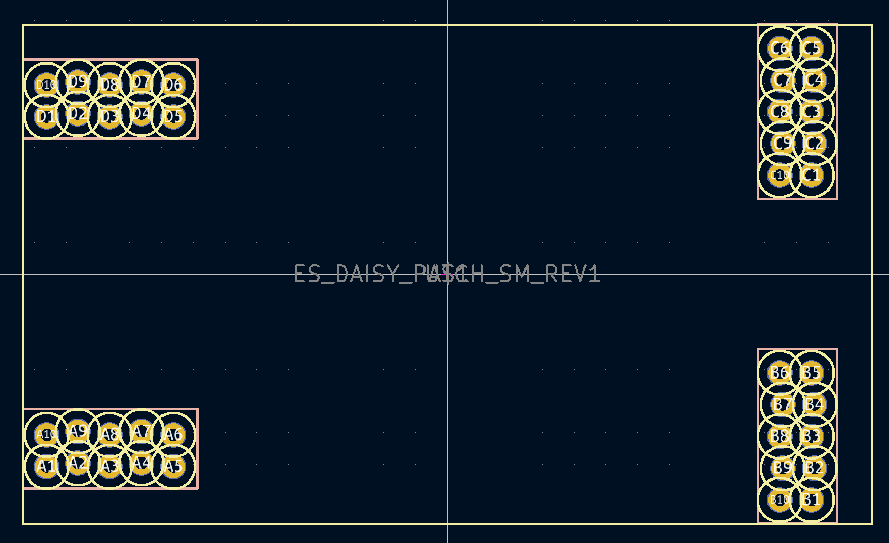
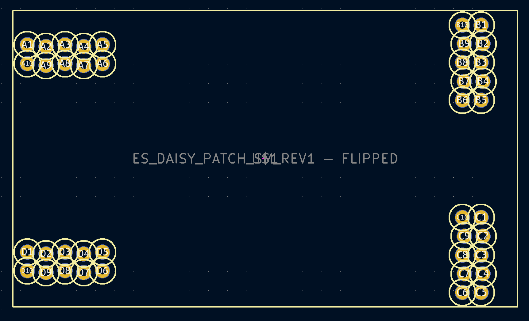
The KiCad footprint supplied in the design files is flipped so that the main silkscreen side with the pin annotations is the reverse of the pins on the Submodule.
I can see how this came about with the patch.Init() board (the headers for the SM are on the back side of the PCB) but this is possibly needlessly confusing and maybe it’d be better to have the pin annotations in the correct orientation and then flip the footprint to the back layer.